Semiconductor Assembly Equipment | Die Attach | Wire Bonding | Regional Breakdown | April 2026 | Source: WGR
Semiconductor Assembly Equipment Market
Key Takeaways
-
Semiconductor Assembly Equipment Market is projected to reach USD 28.6 billion by 2035 at a 12.8% CAGR.
-
Advanced packaging (2.5D/3D, fan-out) and hybrid bonding equipment are the dominant structural growth drivers.
-
Chiplet integration and heterogeneous integration are gaining traction among OSATs and IDMs.
-
Besi, ASM Pacific Technology, Kulicke & Soffa, Shinkawa, Towa, and Disco lead competitive supply.
-
Asia-Pacific dominates assembly; North America accelerates through domestic chip manufacturing expansion.
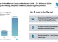
The Semiconductor Assembly Equipment Market is projected to grow from USD 8.2 billion in 2024 to USD 28.6 billion by 2035 at a 12.8% CAGR, driven by the mass-market adoption of advanced packaging equipment across OSAT and foundry sectors, the expansion of hybrid bonding into high-performance computing (HPC) and AI chiplets, and the proliferation of wafer-level packaging (WLP) that directly reduces form factor and improves interconnect density.
Market Size and Forecast (2024-2035)
Segment & Technology Breakdown
What Is Driving the Semiconductor Assembly Equipment Market Demand?
-
Advanced Packaging Investments: Chiplet integration and heterogeneous integration require advanced assembly equipment, with OSATs and foundries investing $10B+ annually in 2.5D/3D packaging capacity for HPC and AI applications.
-
Hybrid Bonding Adoption: Eliminates solder bumps, enabling 10-100x interconnect density improvement, with hybrid bonding equipment critical for chiplet-to-wafer assembly in next-gen CPUs, GPUs, and HBM memory stacks.
-
Die Attach Precision: Advanced die bonders achieve sub-micron placement accuracy, with multi-die packages requiring 3-5 placement steps per device, increasing equipment utilization and demand.
-
Post-Moore’s Law Scaling: As transistor scaling slows, advanced packaging (chiplets, 3D stacking) provides performance gains, with assembly equipment spending growing 2-3x faster than wafer fab equipment (WFE).
KEY INSIGHT
Advanced packaging fabs deploying hybrid bonding equipment report 5-10x interconnect density improvement and 30-50% reduction in power consumption for chiplet-based designs, enabling continued performance scaling beyond traditional node limits.
Get the full data — free sample available:
→ Download Free Sample PDF: Semiconductor Assembly Equipment Market
Includes market sizing, segmentation methodology, and regional forecast tables.
Regional Market Breakdown
Competitive Landscape
Outlook Through 2035
Hybrid bonding equipment adoption, chiplet integration standardization, and advanced packaging capacity expansion will define the semiconductor assembly equipment market through 2035. Vendors investing in sub-micron die placement, high-throughput hybrid bonding, and panel-level packaging (PLP) will capture the highest-margin foundry and OSAT contracts as assembly equipment transitions from back-end afterthought to critical enabler of semiconductor performance scaling.
Access complete forecasts, segment analysis & competitive intelligence:
→ Purchase the Full Semiconductor Assembly Equipment Market Report (2025-2035)
*10-year forecasts | Segment & application analysis | Regional data | Competitive landscape | 350+ pages*
Keywords: Semiconductor Assembly Equipment | Die Attach | Wire Bonding | Hybrid Bonding | Advanced Packaging | Chiplet Assembly | OSAT | Wafer-Level Packaging
© 2025 WiseGuy Reports (WGR) · All Rights Reserved · wiseguyreports.com
All market projections are forward-looking estimates sourced from WGR’s proprietary research reports and subject to revision.